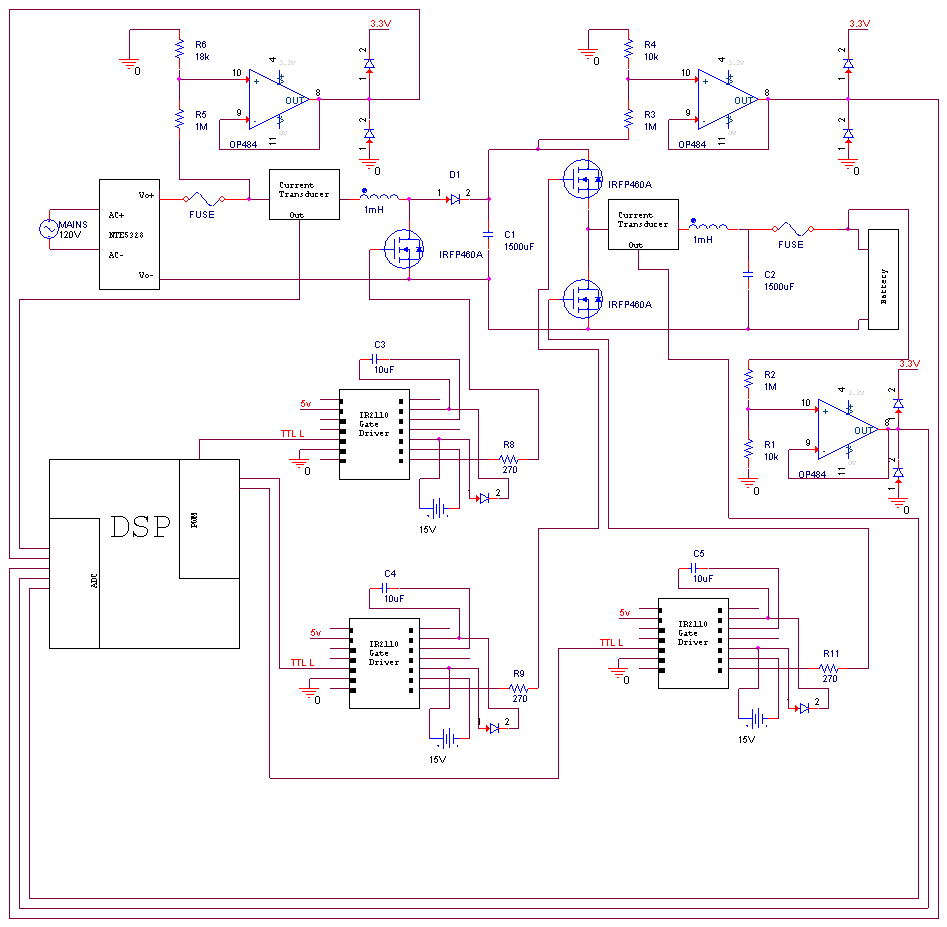
Updates
Matt's Update Page
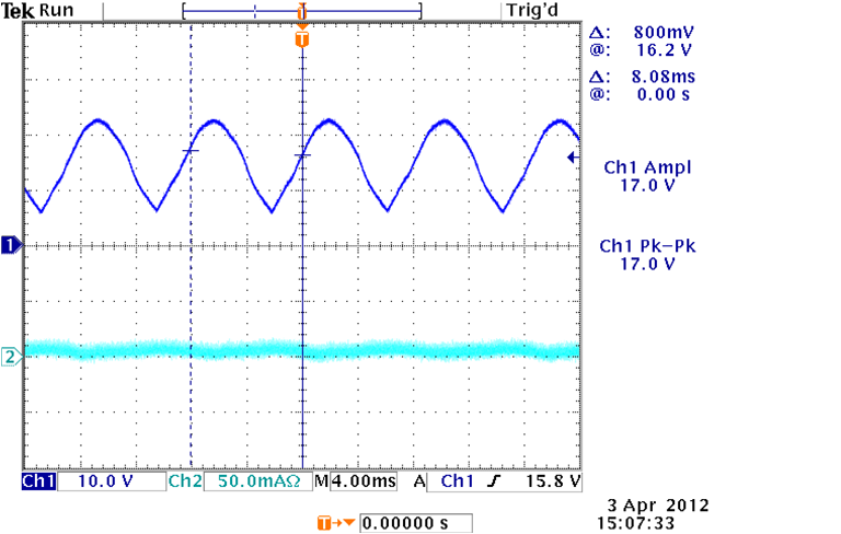
To design a PHEV charging system that will utilize 120V home outlet power we will use multiple power converters to achieve this goal. These high power converters will be responsible for converting AC power to DC and then adjust the DC voltage and current to charge and discharge the battery accordingly. We will be using a NTE5328 rectifier bridge to take the sinusoidal AC input to generate a rectified sine wave. The image below is the output to the boost converter showing the functionality of the NTE5328 rectifier bridge at a lover voltage.
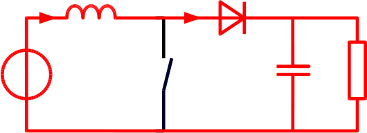
The next stage of power conversion for the design will contain a boost converter, this will serve multiple purposes. One purpose is to improve charging efficiency. While charging, the system will utilize power factor correction achievable with the boost converter. Power factor is the ratio of real power to apparent power. Ideally we want unity power factor or a ratio of 1 for the highest efficiency. The boost converter will align the voltage and current periods; this is achieved with a control algorithm on the DSP. This will be done by sensing the voltage and current of the boost converter and adjusting the duty cycle accordingly. The second purpose of the boost converter will be turning the input sine wave into a recognizable and useable DC voltage. Below is the boost factor design that will we used. The boost converter opperates in 2 stages depending on the on/off state of the IRFP460A N-Type Power MOSFET.
STAGE 1 - In stage 1 current flows through the inductor and energy is stored in it.
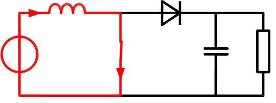
STAGE 2 - The stored energy in the inductor collapses and its polarity changes such that it adds to the input voltage.
Changing the output voltage in this converter is not the main purpose but using the MOSFET to alter the real and apparent power via the inductor is what helps acheve a better power factor. To test the boost converter for proper functionality the equation [ Vo = (1/(1-d))*Vin] will need to be satisfied. Once satisfied we can move from open loop control to a closed loop control system via the DSP.
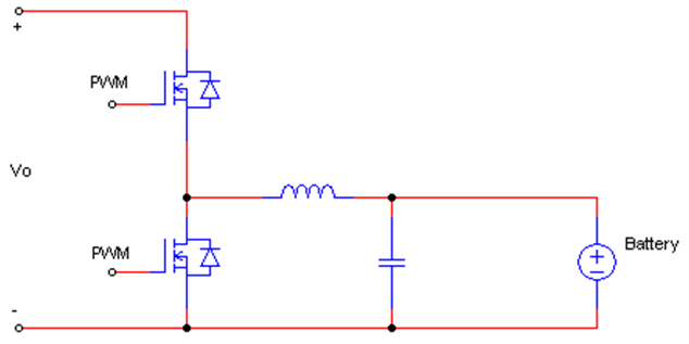
Connected to the boost converter will be a Bi-directional converter this converter will also serve many purposes. This converter is critical to the charging and discharging of the battery safely. The voltage and current exiting the boost converter may not be ideal for proper charging of the battery. When the battery is being charged the Bi-directional converter will act as a buck converter lowering the voltage levels to a safe content value the will properly charge the battery. When the battery needs to be discharged into a load, odds are the load will require a higher voltage than the battery can supply on its own. When discharging the battery the Bi-directional converter will act as a boost converter raising the voltage to a level that will power a load. Below is the Bi-directional converter circuit notice the two IRFP460A N-Type Power MOSFETs that will be controled via the DSP's PWM signal. The two MOSFETS will have complementary duty cycles which will deturmine the current flow and voltage level going to and from the battery.
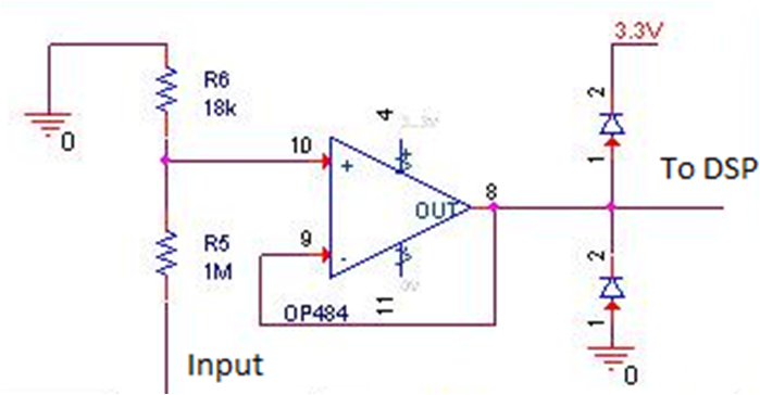
In addition to the main converter systems there needs to be protection circuitry as well as sensing circuitry. In most cases the protection and sensing circuitry are closely connected. To sense the current the L08P050D15 Current Transducer will be used. The current transducer outputs 0-4 volts and the DSP can only take 0-3 volts, so a voltage divider will be used to lover the voltage to the safe level and an Op-Amp will provide additional protection. In order to sense the voltage a similar circuit will be used. A voltage divider connected to an Op-Amp with 2 diodes will be used to isolate the high power circuit from the sensitive DSP board. Also throughout the system fuses will be implemented to further protect the DSP from current spikes. Below in an image of the voltage sensing circuit for sensing the 120V input to the circuit. A voltage devider will lower the voltage to 0-3 volts and the Op-Amp and diodes make sure that the voltage does not go out of that boundry. To calculate the values of the voltage devider the equation [Vout=Vin*(R2/R1+R2)] was used with around a 120V input the values of 1M and 18K were chosen keeping the ratio to a value that will yield a Vout no higher than 3V and the current low enough to use 1/4W resistors.
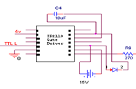
The DSP alone is not capable of providing enough power to drive the IRFP460A N-Type Power MOSFET’s gate so a gate driver will be needed. The IR2110 - 1PBF MOSFET Driver will be used. A voltage supply of 15V will be connected to the gate driver boosting the logic signal from the DSP to a higher level that will properly switch the MOSFET. Below is the setup for the Gate driver. To claculate the bootstrap capacitor the equation [C=((2*Qg+(Igbs{max}/f)+QIs+(Icbs{leak}/f))/(Vcc-Vf-Vls-Vmin))]*15 yields a value of 1.5uf A 10uf capacitor was chosen as the bootstrap for the gate driver. The gate resistor is calculated using the following calculations [Ig=Qg/Ts],[Ig(avg)=Ig/2],[Rg = Vg/ Ig(avg)] a gate resistor (Rg) value of 270 was chosen.
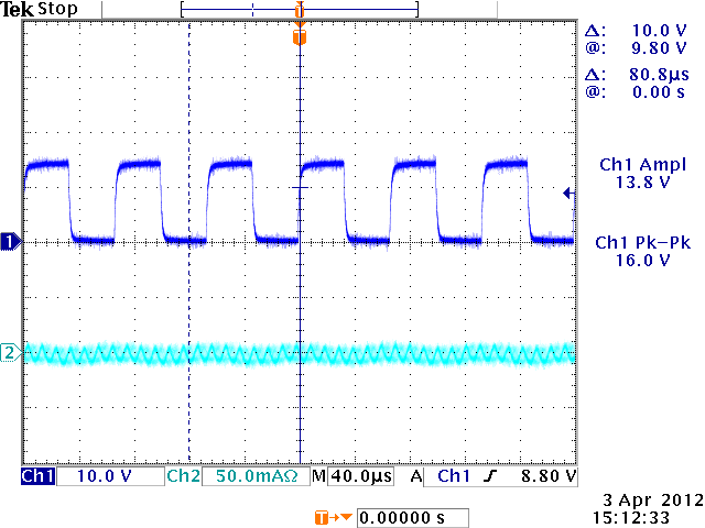
Below is the scope output of the gate driver with a 50% duty cycle in our open loop system. There is roughly a 15V square wave signal that will be driving the MOSFET.
All these parts come togeather and with the DSP running control algorithms to make the final circuit capable of charging the battery and powering the load.