Designing
8-Bit Microprocessor
Using
VHDL
By
Matt
Headley
Advisor:
Dr. Vinod Prasad
Submitted
November 29, 2005
EE451
Senior Capstone Project
PROJECT SUMMARY
This project is designing an 8-bit microprocessor in VHDL. The processor that will be designed will closely resembly the functionality of an 8051. All of the functionality will come from the VHDL code that is written except for the A/D converter that will be interfaced with the FPGA on the Altera UP2 development board. The processor will have most all of the arithmetic and logic functions that are on an 8051. It will also implement timer functionality. There will also be interrupts designed into it as well if time permits.
FUNCTIONAL
DESCRIPTION
Objectives:
The scope of this project is to design an 8 bit microprocessor using VHDL. The design would then be implemented by putting it on an FPGA. The preliminary goal will be to get several commands to work such as mov and add instructions. The desired instructions to be executed and the data to be operated on should be given to the system as inputs. The result of the executed instructions should be the output. After testing the individual parts they will then be combined to test functionality. The final goal is to program an FPGA with the VHDL that is written.
Overall System Description:
The FPGA, once programmed, should behave much the same as an actual microprocessor. This includes an ALU, working registers, and memory. Each part will be designed separately and tested for functionality. After all parts are working they will be combined together forming a simple microprocessor. Figure 1 shows the basic high-level block diagram of the system.
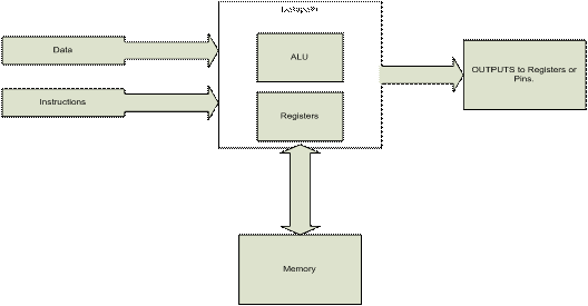
Figure 1 High-level Block Diagram
Figure 1 shows the basic parts that will be designed. The inputs and outputs will be going into and coming out of the FPGA. The registers, ALU, and memory will actually be programmed on the FPGA. The individual parts will be designed separately and then integrated into one system by the use of components or packages in VHDL.
Inputs and Outputs:
It is not decided yet how the final implementation will take in the inputs. To begin with it will simply use different lines high or low to indicate what section is being tested. The instructions will be handled in the same manner. The data that will be operated on will be fed directly into the simulation to begin with. Later different implementations for data and instruction input will be explored such as loading from an EPROM. The outputs will either be the results that are stored in the various registers or various pins will be examined for the expected behavior.
Operations:
There will be several different executable instructions available. The number of them will depend on time constraints and the degree of success with implementing the preliminary instructions. The first instructions that will be implemented will be mov and add. Later additions would possibly include compare instructions, various jumps, logic functions, and other arithmetic operations.
SYSTEM BLOCK
DIAGRAM
Introduction:
This project is to
design an 8 bit microprocessor using VHDL.
The design will first be completed and simulated. Once the simulation proves successful the
VHDL will be put onto a FPGA. The Altera UP2 Development Board includes the FLEX10K FPGA that
will be used. The goal will be to design
a microprocessor that is similar to an 8051.
The desired instructions to be executed and the data to be operated on
will be given to the system as inputs. The result of the executed instructions
will be the output. After the individual
parts are tested they will then be combined to test functionality.
Overall System Description:
The FPGA, once programmed, should behave in much the same way as an actual microprocessor. This includes an ALU, working registers, and memory. Each part will be designed separately and tested for functionality. After all parts are working they will be combined together forming a simple microprocessor. Figure 1 shows the basic high-level block diagram of the system.

Figure 1 High-level Block Diagram
The registers, ALU, and memory will actually be programmed on the FPGA. The individual parts will be designed separately and then integrated into one system through the use of components and packages in VHDL.
ACC and ALU:
The block diagram in Figure 2 shows how the data and instructions are handled in the ACC/ALU module. The Accumulator accepts the data that is to be manipulated. The ALU takes the additional data that will be operated on and the instructions for that data from the system bus. The result of the operations will then be placed back in the Accumulator. The data can only be sent to the system bus from the Accumulator. The ALU can only read the additional data and instructions from the bus and cannot send any information to the bus. This process is shown in a flowchart in Figure 3.
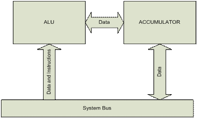
Figure 2 Accumulator and ALU subsystem
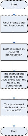
Figure 3 Accumulator and ALU flowchart
Operations:
There will be several different executable instructions available. The instructions that are normally available on an 8051 that I will implement are mov, add, subb, mul, orl, anl, xrl, rl, rlc, rr, and rrc. Later additions may include compare instructions, various jumps, interrupts, and timer functions. The operations will be given an enumerated type as well bit patterns to represent the opcodes. This is illustrated briefly in Figure 4.

Figure 4 Opcode enumeration and bit pattern example
SCHEDULE
|
Week/Date |
Task to be completed |
|
Week 1 |
RAM/memory |
|
Week 2 |
RAM/memory testing with ALU/ACC |
|
Week 3 |
TIMERS |
|
Week 4 |
TIMERS |
|
Week 5 |
TIMERS |
|
Week 6 |
TIMERS |
|
Week 7 |
A/D |
|
Week 8 |
A/D |
|
Week 9 |
Program Counter |
|
Week 10 |
Interrupts |
|
Week 11 |
Interrupts |
|
Week 12 |
Overall control module |
|
Week 13 |
Combining/Testing/Programming FPGA |
|
Week 14 |
Last minute touches |
|
Week 15 |
Presentation |
EQUIPMENT LIST
Altera UP2 Development Board
ADC0801 A/D