Team Member: Matthew Headley
Advisor: Dr. Vinod Prasad
Project: Designing 8 Bit Microprocessor Using VHDL
Objectives:
The scope of this project is to design an 8 bit microprocessor using VHDL. The design would then be implemented by putting it on an FPGA. The preliminary goal will be to get several commands to work such as mov and add instructions. The desired instructions to be executed and the data to be operated on should be given to the system as inputs. The result of the executed instructions should be the output. After testing the individual parts they will then be combined to test functionality. The final goal is to program an FPGA with the VHDL that is written.
Overall System
Description:
The FPGA, once programmed, should behave much the same as an actual microprocessor. This includes an ALU, working registers, and memory. Each part will be designed separately and tested for functionality. After all parts are working they will be combined together forming a simple microprocessor. Figure 1 shows the basic high-level block diagram of the system.
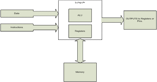
Figure 1 High-level Block Diagram
Figure 1 shows the basic parts that will be designed. The inputs and outputs will be going into and coming out of the FPGA. The registers, ALU, and memory will actually be programmed on the FPGA. The individual parts will be designed separately and then integrated into one system by the use of components or packages in VHDL.
Inputs and Outputs:
It is not decided yet how the final implementation will take in the inputs. To begin with it will simply use different lines high or low to indicate what section is being tested. The instructions will be handled in the same manner. The data that will be operated on will be fed directly into the simulation to begin with. Later different implementations for data and instruction input will be explored such as loading from an EPROM. The outputs will either be the results that are stored in the various registers or various pins will be examined for the expected behavior.
Operations:
There will be several different executable instructions available. The number of them will depend on time constraints and the degree of success with implementing the preliminary instructions. The first instructions that will be implemented will be mov and add. Later additions would possibly include compare instructions, various jumps, logic functions, and other arithmetic operations.