Team Member: Matthew Headley
Advisor: Dr. Vinod Prasad
Project: Designing 8
Bit Microprocessor Using VHDL
Block
Diagram
Introduction:
This project is to design an 8 bit microprocessor using VHDL. The design will first be completed and simulated. Once the simulation proves successful the VHDL will be put onto a FPGA. The Altera UP2 Development Board includes the FLEX10K FPGA that will be used. The goal will be to design a microprocessor that is similar to an 8051. The desired instructions to be executed and the data to be operated on will be given to the system as inputs. The result of the executed instructions will be the output. After the individual parts are tested they will then be combined to test functionality.
Overall System Description:
The FPGA, once programmed, should behave in much the same way as an actual microprocessor. This includes an ALU, working registers, and memory. Each part will be designed separately and tested for functionality. After all parts are working they will be combined together forming a simple microprocessor. Figure 1 shows the basic high-level block diagram of the system.
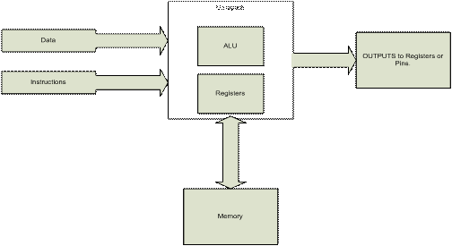
Figure 1 High-level Block Diagram
The registers, ALU, and memory will actually be programmed on the FPGA. The individual parts will be designed separately and then integrated into one system through the use of components and packages in VHDL.
ACC and ALU:
The block diagram in Figure 2 shows how the data and instructions are handled in the ACC/ALU module. The Accumulator accepts the data that is to be manipulated. The ALU takes the additional data that will be operated on and the instructions for that data from the system bus. The result of the operations will then be placed back in the Accumulator. The data can only be sent to the system bus from the Accumulator. The ALU can only read the additional data and instructions from the bus and cannot send any information to the bus. This process is shown in a flowchart in Figure 3.
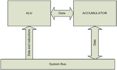
Figure 2 Accumulator and ALU subsystem
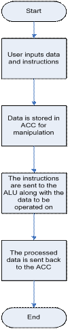
Figure 3 Accumulator and ALU flowchart
Operations:
There will be several different executable instructions available. The instructions that are normally available on an 8051 that I will implement are mov, add, subb, mul, orl, anl, xrl, rl, rlc, rr, and rrc. Later additions may include compare instructions, various jumps, interrupts, and timer functions. The operations will be given an enumerated type as well bit patterns to represent the opcodes. This is illustrated briefly in Figure 4.

Figure 4 Opcode enumeration and bit pattern example