![]()
|
|
|
|
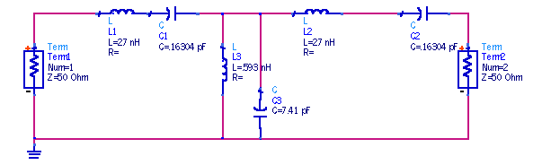
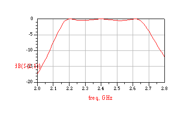
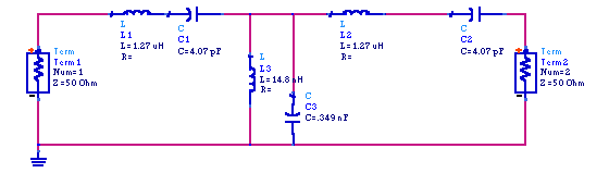
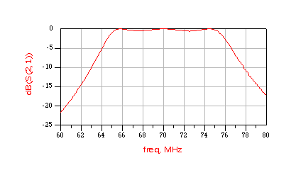
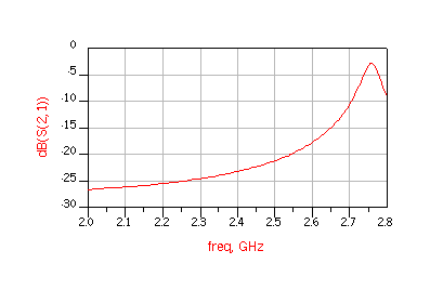
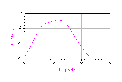
There are two methods of design a band pass filter, image parameter method and insertion loss method. Image parameter method uses several two-port filter sections to provide the desired cutoff frequencies and attenuation characteristics, but do not allow the specification of a frequency response over the complete operating range. The insertion loss method uses a network synthesis technique to design filters with completely specified frequency response. The insertion loss method allows filter performance to be improved in a straightforward manner, at the expense of higher order filter. The task was to design two band pass filters, a 2.4 GHz band pass filter and a 63 MHz band pass filter. The 2.4 GHz band pass filter was to be designed at a center frequency of 2.4 GHz with a bandwidth of 10 MHz and 22 dB attenuation. The 63 MHz band pass filter was to be designed at a center frequency of 63 MHz with a bandwidth of 10 MHz and 22 dB attenuation. For both of the band pass filters the insertion loss method was used. A Chebyshev response was used to satisfy the requirement for the sharpest cutoff. At first, a low pass filter prototype beginning with a series element having a 0.5 dB ripple response was designed. The elements values were determined by using the attenuation versus normalized frequency for an equal ripple filter at 0.5 dB ripple. Then using the element values for the low pass prototype, L1, C2, and L3 were obtained. To make the prototype a band pass filter equations were used to get the value for L1, L2, L3, C1, C2, and C3 (see equations and calculation in Appendix E). For the 2.4 GHz band pass filter L1 was 1.27 µH, which was not able in the market with a self resonant frequency greater then 2.4 GHz. So the logical thing was to design the 2.4 GHz band pass filter with the components able in the market. The specification of the 2.4 GHz were changed, the bandwidth was increased to 500 MHz instead of 10 MHz. After getting the desired values for the inductors and capacitors, for both band pass filters, the circuit was built in ADS (Advanced Design System). The circuits shown in Fig 33 and Fig 35 were simulated. When the desired amplitude responses for the 2.4 GHz and 63 MHz band pass filters were obtained (Fig 34, Fig 36), the 50 ohm transmission lines were added (Fig 37, Fig 39). The 50 ohm lines changed the entire amplitude response of the filter (Fig 38, Fig 40). This happened because the 50 ohm lines have self inductance and capacitance. To get the desired amplitude response the lengths of the 50 ohm lines had to be altered. By altered meaning the length of the 50 ohm lines had to be in increased or decreased. With the help of the optimization tool in ADS the 50 ohm lines were optimized shown in Fig 41 and Fig 42. But was a tradeoff between the length of the 50 ohm lines and the loss. By simulating in ADS is was determined that decreasing the 50 ohm lines the loss was at minimal, but the problem was that the 50 ohm lines had to be long enough for an inductor or capacitor to be soldered on. After the best possible result was obtained, a layout was created in ADS (refer to Appendix F) and a mask was created with the help of Technicraft, to fabricate the board for testing. This process was done for both band pass filters. After fabricating the 2.4 GHz and 63 MHz band pass filter the components, inductors and capacitors, were solder on to the board. After soldering the components the band pass filters were tested using the Network Analyzer in the RF lab. At first the results of the 2.4 GHz band pass filter was not as expected, the loss was significant compared to the simulated result. So we went back to the soldering table and checked if all the capacitors and inductors were connected, while debugging we found some of the inductors were not connected properly and another problem was the grounding. The circuit is so small that it’s fragile. We needed to add a metal base to the circuit for better grounding, but due to lack of time we weren’t able to get the base. These were the reason the result weren’t close to the results obtained in simulation. After debugging, the inductors were re-soldered on the board and retested. This time the result was closer to the simulated result, but there was a different between them (Fig 43). The different was 7.973 dB. This was because of the human error involved in soldering the components and improper grounding. We learned our lesson and when it came to soldering the 63 MHz band pass filter we made sure all the components were soldered on correctly and then tested the filter. The result was not as accurately as the simulated result, again due to the error involved in soldering the components and improper grounding, but the result was acceptable and the difference between them was 2.65 dB at 61 MHz and 5.021 dB at 66 MHz see Fig 44.
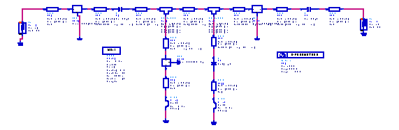
Figure 33 2.4 GHz and 63 MHz band pass filter
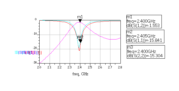
Figure 34 Simulated response of 2.4GHz band pass filter in ADS
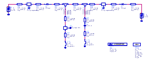
Figure 35 63 MHz band pass filter
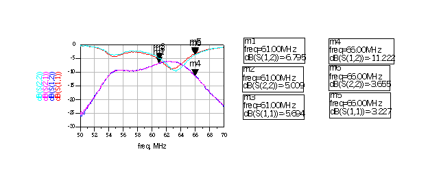
Figure 36 Simulated response of 63 GHz band pass filter in ADS
Figure 37 2.4 GHz band pass filter with the 50 ohm transmission lines
Figure 38 Result of 2.4 GHz band pass filter after adding the 50 Ohm lines
Figure 39 63 MHz band pass filter with 50 Ohm transmission lines
Figure 40 Simulation result of 63 MHz band pass after adding the 50 ohm lines
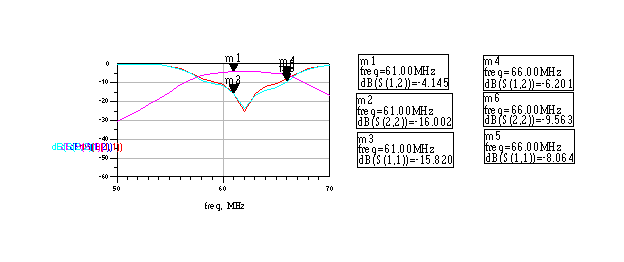
Figure 41 Simulation result of 2.4 GHz band pass filter after optimizing in ADS
Figure 42 Simulation result of 70 MHz band pass filter after optimizing in ADS
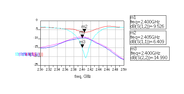
Figure 43 Final result of 2.4 GHz band pass filter
Figure 44 Final result of 63 MHz band pass filter |
|
|