Introduction
Oscillators are the
most important components in modern wireless communication systems. They establish transmission and reception
frequencies for all wireless devices including cellular telephones, radios,
TVs, and satellites. There are several
types of oscillators that are used in commercial and military systems. The most common type of oscillator used
today is the Voltage Controlled Oscillator (VCO). VCOs that are tunable over an octave[1]
frequency range are available commercially.
The distributed
amplifier (DA) is a type of amplifier that can be designed to operate over an
extremely wide frequency range. The
focus of this research project is to examine the feasibility of using a DA as
the basis of a VCO. If the DA proves to
be a viable base for a VCO, VCOs that are tunable over a decade[2]
could then be developed. A DA based VCO
has not yet been successfully implemented.
The goal of this project is to
design a DA based VCO that can be tuned over some span of frequencies within
the range of 1 to 3 GHz. The VCO output
power must be stable over its entire tuning range and should have an output
impedance of 50W. The top-level design of the VCO is shown in
Figure 1. The DA and the Tunable
Bandpass Filter (BPF) are subsystems that are being designed specifically for
this application. A Power Divider and
Feedback Amplifier are being outsourced.
The project is therefore divided into two subsections. Each subsection is then divided into two
parts, making four sections total. Two
members of the student team are working on the BPF design and incorporating the
Feedback Amplifier into the overall subsystem; the other two members of the team
are working on the DA design and incorporating the Power Divider into the
overall subsystem. Each component will
be tested independently and then be interconnected within their specific
subsystem for testing. The two
subsystems will then be connected once again for testing with the ultimate goal
of building the entire VCO circuit on one microstrip layout. This report will contain the entire system
specifications, complete system schematic, each component design and test
results, the interconnectivity results, further work suggestions, and some
comparisons to previous work done.
System
Specifications
·
Output
Frequency Range: 1.8 to 2.5 GHz
·
Output
Power: Stable
over whole
frequency range
·
Output
Impedance: 50W
·
Tuning
Voltage: 0 to
-30 V
·
Biasing
Voltage: 20 V DC
System Layout
Figure 1:
Simplified System Layout
Subsystem Design:
Distributed Amplifier:
The concept in the senior capstone project is testing the feasibility of using a distributed amplifier to increase the bandwidth at which the VCO can tune. Distributed amplifiers are attractive in a project such as this because the maintain high gain while providing a large bandwidth of operation.
The distributed amplifier (DA) works by cascading transistors connected to drain and gate lines made up of inductors and capacitors. The current will interfere in a de-constructive way towards the gate and contructively interfere, or add, and produce power across the output resistor. By increasing the number of transistors, one can increase the current that is produced, thus increasing the power.
Because the model for a transmission can be interpreted as a T-model of two inductors, each of one half value, and a capacitor. Therefore, modeling the gate and drain lines with components gives two advantages:
1.) First it offers more flexibility because one can tune the values of the lines according to his/her needs.
2.) Secondly, anything that is made up of components can be redesigned as microstrip lines for easy fabrication instead of soldering tiny components.
The Distributed Amplifier discussion will be broken down into the steps taken to design and implement the DA.
· Components used
· K- derived
· M- derived
· Microstrip implementation
· Nonlinear model
Components Used
The first task in the design of the distributed amplifier is the research of the components to be used in the design. All of the components must operate over the VCO’s passband. Since the gate, drain, and termination will be realized as microstrip lines, the focus was toward finding the ideal transistor to be cascaded, choke inductors, and blocking capacitors.
The
capacitors and inductors brands and values were already known since similar
projects have been constructed in the RF laboratory at Bradley University. A 2400 pF capacitor is the standard used (see
Capacitor Spec Sheet , Appendix A). The choke inductor is also a standard from Coil Craft (22nH). The inductor and capacitor are used in the biasing network (Inductor Spec Sheet, Appendix A).
The VCO was intended to tune over a range of 1 to 3 GHz. Therefore the transistor used need the same operating frequency. After much investigation, a CEL brand transistor was chosen. The NE72218 has the required operating frequency (see NE72218 Spec Sheet, Appendix D).
At high frequencies, the inductor is the equivalent to an open circuit. It will not be and ideal OC though. Therefore the capacitance will become a short circuit to allow for a very low resistance route to ground for the RF signal so it will not load the DC source used.
DC will make the inductor a short circuit so the current will bias the transistor and not enter the RF source.
K-Derived Distributed Amplifier
The chosen amplifier small signal model is able to be simulated using its S-Parameters. These are available at most product’s home pages (www.CEL.com). This is necessary to prove that the actual simulated S-Parameters will match what the spec sheets say it will do. The S-Parameters were downloaded into a *.s2p file and turned into an S-Parameter block on Agilent ADS. The transistor was able then to be simulated. The resultant outputs were very close to the spec sheets readouts (See NE72218 Spec Sheet, Appendix D).
The first modeling of the distributed amplifier has to be done in what is called K-Derivation. This model incorporates parasitic capacitance Cpad into the design as a physical capacitor. This is done so that values of input capacitance and output capacitance can be calculated.
Cpad + Cout = Cin
From the capacitance found, the equivalent inductance of the gate line inductance, drain line inductance, and the frequency cut-off can then be derived.
Ö(L ¤ C) = 50 W Þ because the desired normalization is 50 W standard
Lg = (50)^2 * Cin
Ld = (50)^2 * (Cout + Cpad)
It is necessary to use the average value of the input and output capacitance . This is obtained by creating the necessary formulae in Agilent ADS and simulating over the operating frequencies. Figure 2 and Figure 3 show the ADS computations to acquire Cin and Cout averages from the Y-Parameters.
From the average value computations :
Cin = 7.790 e-13 F
Cout = 4.011 e-13 F
Cpad = 3.779 e-13 F
Lg = Ld = 1.9475 nH
Figure 2. Frequency v. Y-Parameters
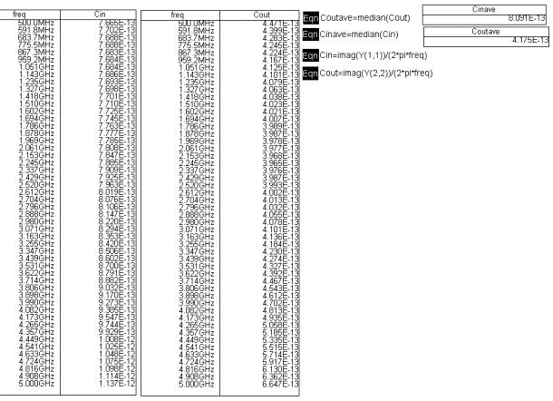
Figure 3. Frequency v. Capacitance
It is necessary to minimize phase shifting within the device so the phase of the output is as close to the input as possible. Capacitance is known for causing phase shift. If an equivalent inductance is put into place, it will eliminate the effect. Therefore when the gate and drain terminations are created, the optimal design would to incorporate a m-derived termination. M-derived terminations make use of equivalent inductance, not capacitance. It will also be seen later that the optimal DA design will also be m-derived. It is just necessary for the initial design to be k-derived because it allows the values of the gate and drain line inductance to be calculated. Figure 4 shows the ADS terminations.
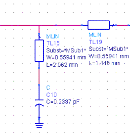
Figure 4. M-Derived Termination
Cterm = (m* C) ¤ 2
Lterm1 = (m* l) ¤ 2
Lterm2 = [(1 – m^2)*L] ¤ 2m
Where m is the constant of derivation. The optimal value for m was stated as 0.6.
Now with the values of all components needed for the design, the question of gain comes to mind. The project would need moderate gain, maximally stable, over the passband. In order to see the resultant gain, say, with three amplifiers cascaded, Agilent ADS would be used to simulate the circuit ( see Figure1 , Appendix A ). The gain properties of a distributed amplifier follow increasing the number of transistors will effectively increase the current and create more gain while decreasing the bandwidth.
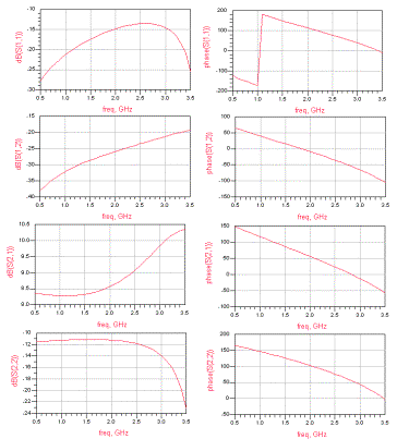
Figure 5. M-Derived S-Parameters
It was noted that the gain was neither flat nor 10dB. 10 dB had been stated earlier by Dr. Shastery as a starting point. The maximum flatness is necessary to maintain a stable output amplitude over the desired frequency.
The problem of passband flatness is because the inductance used was an averaged value.
Therefore it is not the optimal inductance to eliminate the capacitance. When the frequency changes, the impedance changes since the capacitance was not taken care of. As the impedance changes, the amount of current increases or decreases changing the power gain at the output. It was decided to be dealt with later when the design went to microstrip implementation. The drain and gate lines would then be adjusted in length to tweak the values to get maximum flatness.
With addition of a fourth transistor, an increase was seen in the gain. It now was greater than or equal to 10 dB at all frequencies. Also noted was that the phase shift of the gain of S21 decreased rather linearly which means most of the problematic capacitance has been eliminated.
M-Derived Distributed Amplifier
The m-derived design eliminates the padding capacitance with yet another inductor connected directly to the drain of each transistor. The drain values also change with respect to the m constant. The gate values remain the same as for the k-derived DA.
Ldm = m*Ld
Lm =
[Ld (k – m^2)] ¤
4m Þ inductance that eliminates
the padding capacitance
Where k = [m (Cout + Cpad)] ¤ Cout.
Next, the components’ values were changed from the k-derived model and re-saved as the m-derived model on Agilent ADS (see Figure 2, Appendix A). The design was simulated and it was found that the gain matched the S21 of the k-derived model. The phase though was a little more linear. This would be because Cpad was now gone.
Figure
6. M-Derived DA S-Parameters
The m-derived model will now be converted to micro-strip lines to create the physical gate and drain paths. When this happens, the passband gain can be made maximally flat by simply adjusting thelengths of the lines in the gate and drain. The conversion is shown below:
***note – These equations are to be used for short lengths only.
Length of an inductor:
(f*lgl*L)/ZoL
Length of a capacitor.
F*lgl*Zoc*C
Where:
· f represents the highest operating frequency
· lgl represents the wavelength inside the microstrip at the largest frequency (obtained by
MSTRIP)
· ZoL is a higher impedance that 50W. For instance, 80W is a typical impedance of an inductive
line
· ZoC is a lower impedance that 50W. For instance, 30W is a typical impedance of a capacitive
line
As a check, the value of the inductance may not be greater than lgl ¤ 7. This is due to the fact that if it is greater, the wavelenght will not travel properly inside a line of certain impedance and length.
From MSTRIP;
(for Zo = 80W)
Width of line (W) = 0.55941 mm
leff = 65.956 mm
Then, for Ld = 1.168 nH;
Length of drain = 2.889 mm
For Lg = 1.9475 nH;
Length of gate = 4.817 mm
For Lpad = 0.091638 nH;
Length of pad = 1.615 mm
From MSTRIP;
(for Zo = 30W)
Width of line (W) = 26.382 mm
leff = 62.594 mm
All
m-derived component and termination lengths are now able to be computed. All
biasing networks will remain in lumped elecment form.
The circuit is first simulated without the biasing networks.
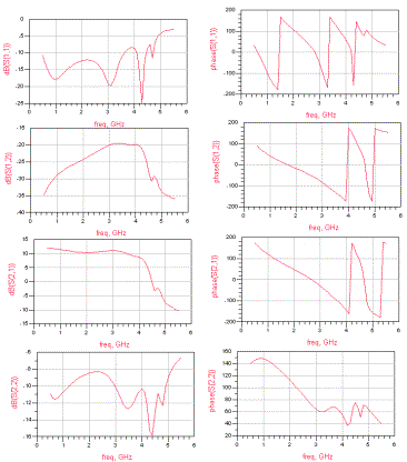
Figure 7
The response of S21 is very similar to the lumped element model. The gain seems to be adequate, yet not flat. Optimal values of drain and gate lengths will have to be found.
After connecting the biasing networks, non-linearity was introduced. This is because there has to be a DC source connected. And biased. In order to see what Vgs needs to be, the DC/IV curves have to be generated. It is possible to do so on ADS on a DC simulation of Ids vs Vds. The nonlinear model will allow this simulation to occur over the large signal model.
For the non-linear model, the
S-parameter block is replaced by the TOM model (See Figure 3, Appendix A).
The non-linear TOM model is necessary because when the amplifier is used in an oscillator, it becomes unstable(nonlinear). Therefore the non-linear simulation must be done to see how it is going to react. Model parameters were avialable at the CEL’s website. Shown in Figure 8, a current meter was placed to measure the Ids to plot agianst VGS.
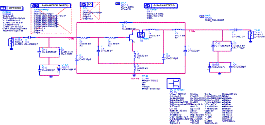
Figure
8. Agilent ADS TOM Model Simulation
The results seem very wrong. In theory they should at least come close to the S-parameter simulation of just the transistor. The S21 of the system seems to be very distorted. Obviously in an amplifier system, the gain should be maximally flat and positive. The gain of this system is negative. Attenuation is not desirable.
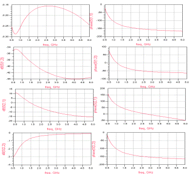
Figure 9. Nonlinear Simulation Agilent ADS
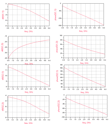
Figure 10.
NE77218 S-Parameters
The reason for the inconsistancy of the S-Paramters is
unknown. The model has been inspected
several times by many people. When
contacted, CEL representative Mr. Kodani stated that the chief modeler had
recently quit. This leaves us with no
other alternative but to use the previous DA design in the interconnectivity test. It is far too late to try to implement a new
transistor because it would take too much time.
Power
Divider:
The power divider is used to split the power coming out of the distributed amplifier into two equal outputs. One of the outputs from the power divider is the output of the VCO. The other output is sent into the feedback loop through the gain amplifier.
A lot of time was spent searching for a power divider that worked in the frequency range of the VCO. A two-way surface mount power divider with a low insertion loss had to be chosen. The power divider that was chosen for this project was the 4A1305 from Anaren, which has a frequency range of 1.4-2.6 GHz.
Calculations were done on the mstrip.exe program on the h-drive to determine the dimensions of the microstrip lines for the input and outputs of the power divider. Simulations were then done on the Agilent Technologies ADS software to determine the s-parameter characteristics of the power divider. The phase balance, magnitude balance, and insertion loss were determined from these simulations. The phase balance is calculated by subtracting the phase of S21 from the phase of S31, and should be equal to zero. As can be see in Figure 11, the phase balance is zero. The large spike in the phase balance plot is due to the jump from negative to positive phase in the plots of S21 and S31, it is also out of the desired frequency range so it can be ignored. The magnitude balance is determined the same way as the phase balance but instead uses the difference in the magnitudes of S21 and S31. The magnitude balance is shown in Figure 11, the magnitude balance should also be zero and it is very close to zero in the desired frequency range of 1.0-3.0 GHz in the plot of magnitude balance below.
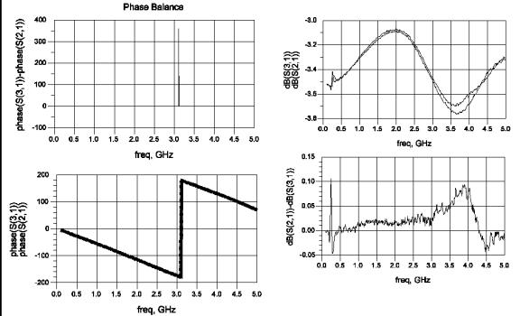
Figure 11. Plots to Show Phase Balance
(left) and Magnitude Balance (right)
The insertion loss of the power divider was also determined from the s-parameter plots. This was also found from the plot of S21 and S31 and compared to the insertion loss plot from the data sheet (see appendix D, data sheet 2). The insertion loss was found by drawing lines up from the points were the desired frequency range starts and ends. The points where the lines crossed the curve were located at around 3.2 dB. Since the actual gain of the power divider should be 3.0 dB, we subtract 3.0 dB from 3.2 dB to get a maximum insertion loss of about 0.2 dB. This was then compared to the data sheet to find that they match.
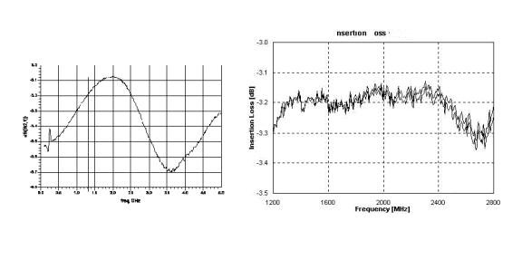
Figure 12. Plots of Insertion Loss
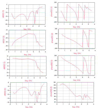
Once the simulations were completed a microstrip layout for the power divider was constructed. First the simulation layout was made in ADS, next a printout of the layout was sent to the CAT Imaging Lab so a mask could be made. The mask was then used to make the microstrip circuit in the Fabrication Laboratory. The power divider component was soldered onto the board and then tested using the HP8722C Network Analyzer. The results of these simulations are shown in Appendix B.
Comparing the magnitude plots of S21 and S31 it can be determined that the magnitude balance from the experimental data is equal to zero since the two plots are the same. Since the phase plots of S21 and S31 are also the same, the phase balance is equal to zero.
Any differences between the experimental plots and the theoretical plots were caused by errors in the microstrip fabrication and quality of connections in the physical circuit.
Gain Balancing:
Gain balancing is essential to the VCO circuitry. Within the feedback loop of the VCO the overall gain must be unity. The feedback loop is where the output of a system is feed back into the system’s input. For a VCO, this is done with the power divider discussed previously. One output from the power divider serves as the VCO system output, the other output from the power divider becomes the start of the feedback loop (see Figure 1). Gain is expressed as the output voltage or power, as in this case, divided by the input voltage or power, as in this case. For unity gain this value needs to be 1, or the output must equal the input in value. Since RF applications deal in Decibels (dB), our unity gain needs to be 0. Some equations needed are as follows:
Gain = (Power out) / (Power in)
Gain (dB) = 20 log [(Power out) / (Power in)]
The reason the gain in dB will be 0 for unity is because the log of 1 is 0.
Gain balancing is necessary because some components will increase the gain of the signal and some components will decrease the gain. The Distributed Amplifier will increase the gain from 0 dB to 10 dB, thereby giving the signal a power level of 10 dB. The power divider will then decrease the gain by 3-5 dB, thereby decreasing the signal power level by the equivalent value. The tunable bandpass filter will then decrease the signal again. Now if we say the initial input to the DA is 0 dB then when the signal return to the DA’s input from the feedback loop, it must once again be 0 dB. This means that if the power divider and tunable bandpass filter combined do not bring the 10 dB output from the DA back down to 0 dB by the time the signal reenters the DA, unity gain is not achieved and there will be no oscillations from our oscillator. This requires a decrease in power level within the feedback loop, or a negative gain, from the gain balancing portion of the system. On the same note, if the power level, or gain, within the feedback loop is less than 0 dB, or negative, then an increase in gain is needed from the gain balancing portion.
Previous work:
In the previous work done by Sunil, the tunable bandpass filter caused the feedback power level to drop below 0 dB. Because of this, an increase in the power level was needed within the feedback loop. He chose to use an amplifier with a positive gain to bring the power level back up to 0 dB. We, as a team, decided to order an amplifier as well because we started out using the same tunable bandpass filter design. This is not the case and will be discussed later.
Current team’s work:
The amplifier chosen was a GALI-3 from Mini-Circuits (see appendix D, data sheet 3). While the amplifier was on order the Scattering Parameters (S-parameters) were obtained from Mini-Circuits website (http://www.minicircuits.com). The S-parameters are shown below in Table 1.
|
Freq |
|
S11 |
|
S21 |
|
S12 |
|
|
S22 |
|
|||
|
(MHz) |
(Input Return
Loss) |
(Power
Gain) |
(Isolation
Out/In) |
(Output
Return Loss) |
|||||||||
|
|
dB |
Mag |
Ang |
dB |
Ang |
dB |
Mag |
Ang |
dB |
Mag |
Ang |
||
|
100 |
-28.31 |
0.04 |
129.62 |
22.25 |
174.88 |
-24.76 |
0.06 |
-0.20 |
-33.17 |
0.02 |
-176.27 |
||
|
200 |
-25.44 |
0.05 |
121.54 |
22.16 |
169.66 |
-24.06 |
0.06 |
0.66 |
-30.94 |
0.03 |
-176.36 |
||
|
400 |
-21.55 |
0.08 |
96.27 |
21.99 |
160.63 |
-23.92 |
0.06 |
0.35 |
-30.65 |
0.03 |
-176.06 |
||
|
600 |
-18.42 |
0.12 |
81.49 |
21.70 |
150.82 |
-24.06 |
0.06 |
-0.48 |
-29.5 |
0.03 |
-175.92 |
||
|
800 |
-16.58 |
0.15 |
71.48 |
21.37 |
142.05 |
-24.09 |
0.06 |
-1.42 |
-27.35 |
0.04 |
-177.16 |
||
|
1000 |
-15.19 |
0.17 |
62.50 |
20.99 |
133.66 |
-24.04 |
0.06 |
-2.32 |
-26.07 |
0.05 |
-178.72 |
||
|
1200 |
-14.25 |
0.19 |
54.52 |
20.58 |
125.57 |
-24.03 |
0.06 |
-1.87 |
-25.01 |
0.06 |
-179.91 |
||
|
1400 |
-13.55 |
0.21 |
47.17 |
20.16 |
118.23 |
-24.06 |
0.06 |
-1.96 |
-24.14 |
0.06 |
178.19 |
||
|
1600 |
-12.97 |
0.22 |
39.78 |
19.78 |
111.51 |
-24.10 |
0.06 |
-2.57 |
-22.92 |
0.07 |
176.26 |
||
|
1800 |
-12.48 |
0.24 |
32.86 |
19.37 |
104.51 |
-24.10 |
0.06 |
-2.00 |
-22.10 |
0.08 |
174.61 |
||
|
2000 |
-12.13 |
0.25 |
26.09 |
18.99 |
98.16 |
-24.37 |
0.06 |
-3.28 |
-21.6 |
0.08 |
173.49 |
||
|
2200 |
-11.81 |
0.26 |
20.10 |
18.59 |
92.03 |
-24.28 |
0.06 |
-3.17 |
-20.93 |
0.09 |
172.38 |
||
|
2500 |
-11.49 |
0.27 |
10.09 |
18.01 |
83.38 |
-24.35 |
0.06 |
-3.19 |
-20.73 |
0.09 |
171.12 |
||
|
2800 |
-10.95 |
0.28 |
1.30 |
17.51 |
75.24 |
-24.58 |
0.06 |
-4.02 |
-20.35 |
0.10 |
169.73 |
||
|
3000 |
-10.82 |
0.29 |
-4.71 |
17.22 |
69.85 |
-24.69 |
0.06 |
-5.16 |
-20.22 |
0.10 |
167.80 |
||
Table 1. S-parameters of the GALI-3
amplifier
Source: Mini-Circuits
Website: (http://www.minicircuits.com/cgi-bin/amplifier?model=GALI-3&pix=df782.gif&bv=4)
Creating a component:
Using the S-parameters obtained from Mini-Circuits, shown in Table1, an .S2P file was created. This is a type of file used in the Agilent ADS simulation software for designing RF circuits. This file is recognized as the S-parameters for a 2 port network (a component with one input and one output), which is the case for an amplifier. The .S2P file is shown in Figure 13.
#GHZ S dB R 50 !freq dB(S11) ang(S11) dB(S21)
ang(S21) dB(S12) ang(S12) dB(S22) ang(S22) 1.0 -15.19 62.50 20.99
133.66 -24.04 -2.32
-26.07 -178.72 1.2 -14.25 54.52 20.58
125.57 -24.03 -1.87
-25.01 -179.91 1.4 -13.55 47.17 20.16
118.23 -24.06 -1.96
-24.14 178.19 1.6 -12.97 39.78 19.78
111.51 -24.10 -2.57
-22.92 176.26 1.8 -12.48 32.86 19.37
104.51 -24.10 -2.00
-22.10 174.61 2.0 -12.13 26.09 18.99
98.16 -24.37 -3.28
-21.60 173.49 2.2 -11.81 20.10 18.59
92.03 -24.28 -3.17
-20.93 172.38 2.5 -11.49 10.09 18.01
83.38 -24.35 -3.19
-20.73 171.12 2.8 -10.95 1.30 17.51 75.24 -24.58 -4.02
-20.35 169.73 3.0 -10.82 -4.71 17.22 69.85 -24.69 -5.16
-20.22 167.80
Figure 13.
S-parameter file (.S2P) for the GALI-3 amplifier from Mini-Circuits for use
with Agilent ADS simulator. The
frequency range of use to us is from 1GHz to 3GHz.
In the Schematic Capture window of Agilent ADS, within the “Component Palette List”, “Data Items” was selected. Within the “Data Items” component list is a button marked “S2P: 2-port S-parameter”. After selecting and placing the generic component in the schematic capture window, double clicking on the component and searching through the “brows” selections lead to the desired .S2P file. After clicking “OK” the .S2P file was linked to the generic component (see Figure 14). Simulations were then run and output S-parameter graphs were obtained (See Figure 15). When compared to the S-parameter graphs in the GALI-3’s data sheet (see appendix D, data sheet 3), the graphs are identical in the 1GHz to 3GHz range. This was expected because the S-parameter values used in the .S2P file are the exact same S-parameters obtained from the manufacturer, therefore the graphs should be exactly the same as well.
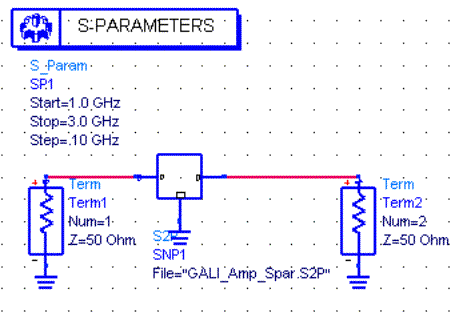
Figure 14. Generic component in schematic capture window of Agilent ADS simulator, with the link
to the GALI_Amp_Spar.S2P file
shown in Figure 13.
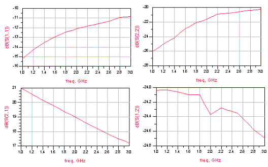
Figure 15. GALI-3 amplifier S-parameters obtained from an Agilent ADS
simulation using
S-parameter
values from the manufacturer.
Knowing that the simulated S-parameter graphs match those from the manufacturer proves that ADS will provide an accurate representation of how the actual amplifier will function. The next work done was the amplifier biasing network.
Amplifier Biasing Network:
The amplifier biasing network is a circuit containing capacitors, inductors, and resistors. The network is needed to apply a D.C. voltage to the amplifier in order for the amplifier to work properly.
A schematic of a typical amplifier biasing network is shown in Figure 16.
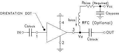
Figure
16. Typical amplifier biasing network.
Capacitors:
In the schematic shown in Figure 16 there are two Cblock components. These are known as blocking capacitors. Their job is to block D.C. voltage and current from getting into the RF signal. A capacitor is seen by a low frequency (D.C.) signal as an open circuit and therefore stops any D.C. signal from passing through. At the same time a capacitor is seen by signals of high frequencies (RF) as a short circuit and therefore allows the RF signal to pass. The equation to show this characteristic is given below in equation (1).
Xc = (1) / (jw*C) (1)
Where:
Xc is the impedance of a capacitor
j signifies the imaginary part of (w*C)
w is the frequency in (radians per second)
C is the capacitor value
From equation 1, it can be shown that if w is very low, say 0 radians per second for D.C., then the impedance will be (1) / (0) which is infinite, open circuit. Thus, no D.C. signal will be passed. But, on the other hand if w is very high, say 6.283 x 10 ^ 9 radians per second (1GHz), then the impedance will be very small, short circuit. Thus an RF signal will pass through.
In the schematic shown in Figure 4 there is one Cbypass. This is known as a bypass capacitor. It works on the same principal as the blocking capacitors (Cblock). Vcc is where the D.C. voltage source is connected. If an RF signal were to enter the D.C. voltage source it would cause some damage. The Cbypass works with the RF Choke Inductor (RFC), to be discussed later, to prevent any RF signal from entering the D.C. source. Because a capacitor is seen by a high frequency signal as a short circuit, any RF signal that may be present at the Vcc side of the Cbypass, will be passed through the capacitor to ground and thus preventing it from entering the D.C. source. Once again, since a capacitor is seen as an open circuit by a D.C. signal, the Cbypass will not allow any D.C. signal to pass to ground.
Inductor:
The RF Choke Inductor (RFC) shown in Figure 16 helps the Cbypass protect the D.C. source from any stray RF signals. This happens because an inductor acts like an open circuit to a high frequency signal and like a short circuit to a low frequency signal. The equation used to show this characteristic is given below in equation (2).
XL = jwL (2) Where:
XL is the impedance of an inductor
J is the imaginary part of (w*L)
w is the frequency in (radians per second)
L is the inductance value
From equation (2), it can be shown that if the frequency is high (RF) then the impedance is high, thus an open circuit. But, if the frequency is low (D.C.) then the impedance is low, thus a short circuit. Therefore, RF signals are stopped but D.C. signals are allowed to pass. This is how the RFC and Cbypass allow the D.C. bias voltage to reach the amplifier, allowing it to work properly, and at the same time protect the D.C. voltage source from damage.
Amplifier:
The triangle shown in Figure 16 represents the amplifier itself. The IN and OUT also shown are the input and output of the amplifier, respectively. The last component in the biasing network is the bias resistor (Rbias).
Bypass Resistor:
The Rbias is needed because the amplifier needs D.C. current as well as D.C. voltage. Current can be found by using equation (3).
I = V / R (3)
Where:
I is the current
V is the voltage (from the D.C. source in this case)
R is the resistor value
The manufacturer, to help with the selection of R, provided a table, shown in Table 2. When using the table, the values for the ERA-3 amplifier, which are identical for the GALI-3 amplifier, were used. From looking at Table 2, it can be seen that the bias current needs to stay the same. Therefore, different voltage levels will require different resistor values.
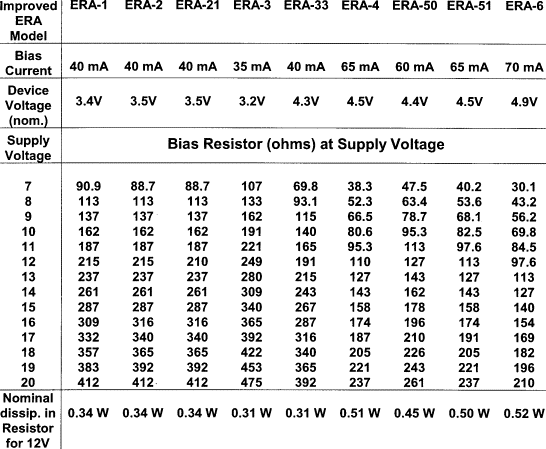
Table 2. Bias
resistor values for various amplifiers and bias voltages, provided by
Mini-Circuits.
The manufacturer also states that for the greatest stability, the highest attainable values for R and Vcc are desired. The RF laboratory at Bradley University has D.C. voltage sources that will provide up to 30 Vdc, therefore the project team decided to use 20 Vdc with a 475W resistor (See Table 2).
Biasing Network Simulations:
The next step is simulating the amplifier biasing network on Agilent ADS. The inductor, capacitors, and resistor used were available components in the RF laboratory. A 2400 pF capacitor is the standard used (see appendix D, data sheet 4). The choke inductor is also a standard from Coil Craft (see appendix D, data sheet 7).
Inductor Model:
An equivalent circuit model for the inductor is shown below in Figure 17. This model when used will provide an accurate simulated representation of how the physical inductor will respond in a circuit. The equations provided in the figure were used to calculate the R and C value shown. The L value was obtained from data sheet 7 in Appendix D at the 1.7GHz frequency point because this is within the range of operation for the VCO. The Q, for use in the equations, was also taken from data sheet 7 in Appendix D at the 1.7GHz frequency point.
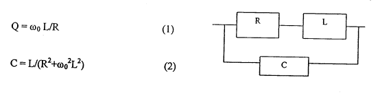
Figure 17.
Equivalent circuit model for the 22nH inductor with equations to use.
Using the equations shown in Figure 17, the resistor and capacitor values are as follows:
R = [(w0) * (L)] / Q => R = 1.1028W
C = L / [ (R^2) + (w0^2) * (L^2)] => C = 4.2563pF
Where:
w0 = SRF from data sheet 7 in Appendix D, which is 3000
L = 26.1nH, from data sheet 7 in Appendix D
Q = 71 from data sheet 7 in Appendix D
The completed amplifier biasing network is shown in Figure 18. When compared to the previous schematic in Figure 16, it can be seen that the RFC is replaced by its equivalent circuit model. It has the appropriate capacitor, inductor, and resistor values from Figure 17. The Rbias from Figure 16 became a 474W resistor because a 475W resistor, decided upon from Table 2, was not available in the RF laboratory.
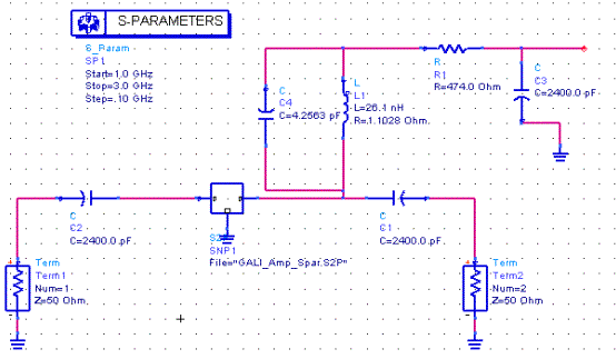
Figure 18. Complete amplifier biasing network from Agilent ADS
simulator’s schematic capture window.
When the circuit shown above in Figure 18 was simulated on Agilent ADS, the S-parameters shown in Figure 19 were obtained. By comparing these S-parameters to those in Figure 15, you can conclude that when the biasing network is included with the amplifier the S-parameters change. The S-parameter of greatest concern for an amplifier is the S21. This is because the S21 of an amplifier is the gain of the amplifier. When comparing just the S21, you can see that the gain dropped by about 4 dB at both the lowest and highest frequencies. This decrease was expected and is fine.
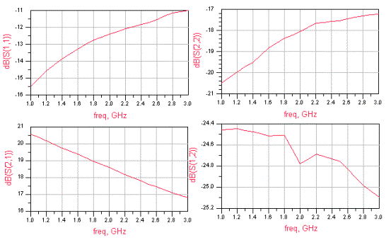
Figure 19. S-parameters for the GALI-3 amplifier and its biasing network obtained from Agilent ADS simulator.
Microstrip Layout:
After completing the simulations without any microstrip lines included, a microstrip layout was designed. A microstrip is just a strip of copper surrounded by nonconductive material on a board. The layout will have microstrip lines separated by blank spaces where components were soldered in. The blank spaces were made exactly large enough for each individual component to be soldered in without causing the microstrip lines to connect underneath the component. A schematic was constructed first using only microstrip lines. The microstrip lines that are labeled with component names represent where the individual components were soldered. These microstrip lines are the proper length of each component and their widths were made very small so when the circuit showed up in the layout window, the lines representing the components could be deleted leaving only blank spaces for component placement. The schematic of microstrip lines is shown in Figure 20 and the microstrip layout is shown in Figure 21.
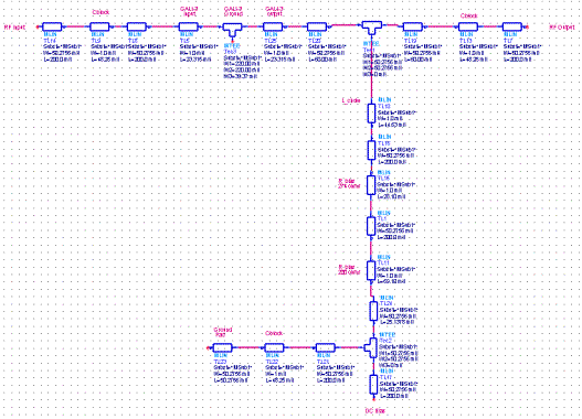
Figure 20.
Schematic used for the microstrip layout for the amplifier biasing network from
Agilent ADS simulator.

Figure 21. Microstrip layout for the
amplifier biasing network at exact size
From Agilent ADS simulator.
As you can see from Figure 21, the circuit is very small and as stated before, each blank space is where a component was soldered into the circuit.
Biasing Network with components and Microstrips:
Once the layout was completed one more schematic was designed and tested. The schematic shown in Figure 22 is the amplifier biasing network containing both the components with their values and the microstrip lines. The results from this simulation were the most accurate way of showing how the amplifier responds when constructed on a microstrip board. The S-parameters from the simulations are shown in Figure 23.
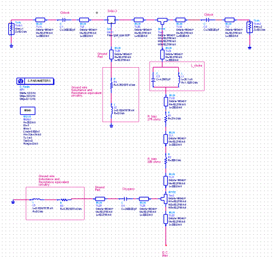
Figure 22. Schematic for amplifier biasing network containing both components and microstrip lines from Agilent ADS simulator.
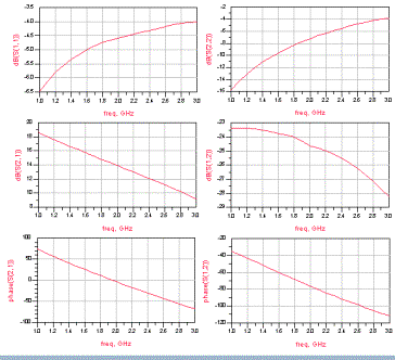
Figure 23.
S-parameters obtained from Agilent ADS simulations of the circuit in Figure 22.
When comparing the S21 in Figure 11 to that of Figure 7, you will notice that the overall gain once again drops. This drop is 1.5 dB from that if Figure 7, thus there is an overall gain drop of 1.9 dB from the manufacturers provided S21 parameter.
Tunable
Filter:
This subsystem is responsible for selecting the actual frequency at which the system will oscillate. In order to perform this task properly, the filter should have a low insertion loss; stable loss over the entire tuning range; consistent phase shift over the entire range; and have a consistent voltage to passband relationship. The work done, by Sunil Modur, toward developing a DA based VCO used a tunable filter that met all the preceding constraints; except it had a very high insertion loss. This problem needed to be resolved in the current design iteration. Research has found that varactor tunable microstrip resonators[3] should have a much lower insertion loss and still have a very stable loss over the entire tuning range.
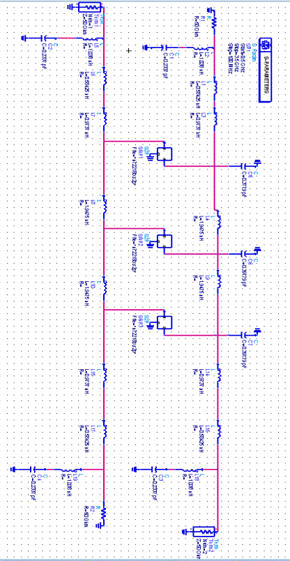
Based on the conclusions drawn from Dr Kapilevich’s work, the double terminated varactor tunable microstrip resonator in series was selected for this project. A top level schematic of this configuration is shown in figure 24 below. This circuit operates by using the variable capacitance inherent in varactor diodes to adjust the resonant frequency of the resonant circuit. The resonant circuit is bounded by a pair of capacitors (C1) followed by symmetric microsrip sections (M1). C1 and M1 work to shape the passband’s width; they also have some impact on the actual frequency range and transmission losses. The varactors (Ct) perform the actual tuning and have a limited effect on the other filter characteristics. The primary resonant strip (M2) has the most influence over where the center of the filter tuning range will be; it also impacts the transmission losses and filter passband width to a small extent.
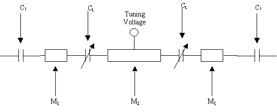
Figure 24: Configuration of a double
terminated varactor with tunable microstrip resonator in series.
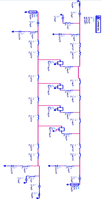
Due to the tremendous complexity of Dr Kapilevich’s design process and a lack of intermediate or direct design equations, the process used to develop the filter for this system was a simulation approach starting with values established in Dr. Kapilevich’s work and systematically modified to have a tuning range centered at 2.0GHz. After obtaining the appropriate center to the tuning range further adjustments were made to minimize the passband width and stabilize the transmission losses for the entire tuning range. Figure 25 shows the design used to establish a tuning range centered at 2.0GHz. Figure 26 shows the simulation results for the transmission characteristics of the filter with Cp varying from 0.2 to 2.0pF. The transmission characteristics show that this filter design should have stable passband loss with a tuning range from about 1.5 to 2.5GHz. The system provided a basis for selecting the components needed to fabricate the device.
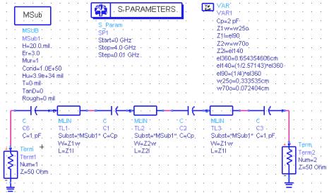
Figure 25. Initial ADS filter design
(used to establish component to
tuning range relationships)
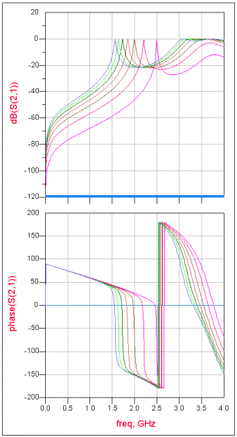
Figure 26. Simulation results for the transmission
characteristics of the
circuit in figure 25 (Cp was varied from 0.2 to 2.0pF)
The varactor (Ct in figure 24) was selected based on its frequency of operation, high Q factor[4], tuned capacitance range, and the availability of a simulation model. The varactor selected was the SMV1405-079 from Alpha Industries (See Data Sheet 5, Appendix D). Similar constraints determined the C1 capacitor (refer to figure 24) used for the filter, only without the need for a detailed simulation model. The capacitor selected was the A2M1 trimmer capacitor from Voltronics (See Data Sheet 6, Appendix D).
The next step in the development of this filter was to construct a detailed simulation model, which will account for most of the parasitic effects associated with using physical components, and optimize the detailed model. The varactor was modeled using the spice model on page three of the data (See Data Sheet 5c, Appendix D). The trimmer capacitor was modeled using an ideal capacitor in series with an inductive and resistive element. The parasitic effects were determined by modeling the long connection on top of the capacitor shown in figure 27. The dimensions measured from the capacitor lead were entered into the self-inductance and AC resistance equations for “a strip of rectangular conductor” (shown below):
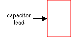
Figure 27. An enlarged picture of the A2M1 trimmer
capacitor.
(with the section modeled as an
inductive and resistive element marked)
Lnh=5.08*10-3*l*[ln((2*l)/(W+t))+dL+(0.223*(W+t))/l+0.25]
Rac=l/(2*d*s*(W+t))
dL=(d/2)*Ö(p/W*t)
d=1/Ö(p*f*m*s)
s=conductivity (S/m)
m=permeability (H/m)
f=frequency (Hz)
l=conductor length (mils)
W=conductor width (mils)
t=conductor thickness (mils)
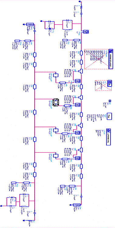
The final of parasitic effects that were modeled in the final design for simulation were those induced by the wire connections through the substrate to ground as well as microstrip thickness changes induced by connections to the surface mount components. These effects can be directly modeled in Agilent ADS; after modeling the parasitic effects some further filter optimization was performed by fine tune adjusting of the microstrip dimensions. The complete subsystem is shown in the appendix C, figure 1. Simulating the complete subsystem in ADS resulted in the S-parameter data displayed in figure 28.
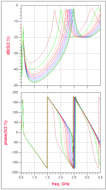
Figure 28. Simulation results for
the transmission characteristics of the
Detailed subsystem circuit (Appendix C Figure 1) Vdc was varied from 0 to 30V
These results show that the fabricated filter should meet the design criteria established for this subsystem. The wide fluctuation in the phase shift for the filter is a source of concern, however this can be taken into account when designing the rest of the system. The next step in the system design was to construct a test filter to verify the simulation data.
The fabrication process includes the following steps:
1) Construct a layout model with ADS.
2) Send model to CAT Image Lab to be developed into a mask.
3) Use the mask to develop and etch the circuit.
4) Send the newly etched circuit to the JOBST Machine Shop to have ground lines drilled.
5) Solder the ground lines, connectors, and various surface mount components.
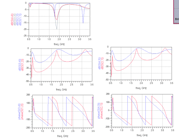
The first test filter constructed did not match the designed dimensions and the test data was far from what was predicted in simulation (See Figure 2, Appendix C). The most probable sources of error for the discrepancies in the data are:
·
Test board to simulation layout
dimension mismatch.
·
Poor connections in test board.
·
Difficulties in setting end
capacitor values.
·
Slight variations in varactor
performance.
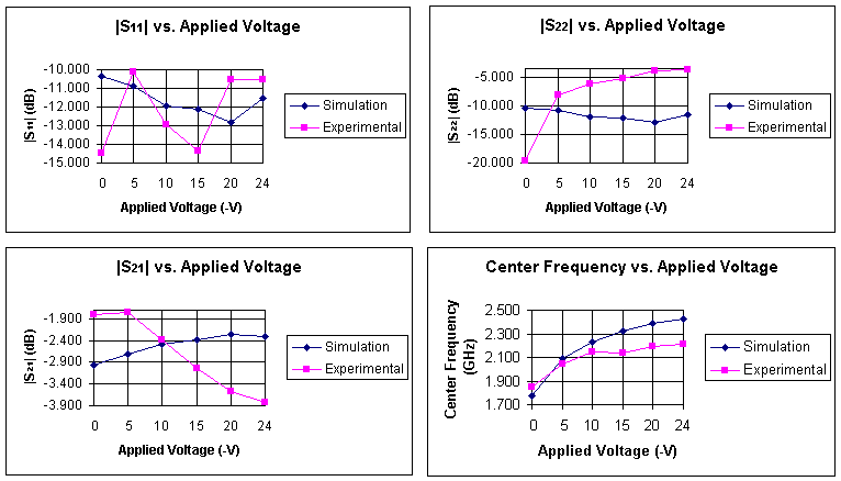
In order to develop more reliable data a new filter was constructed that more closely matched the designed system (the dimensions were still off in many places). As is shown in figure 3 of appendix C the data for the second test filter came very close to the results predicted in simulation. This second test filter had a tuning range that spanned 1.88GHz to 2.66GHz with a transmission loss that varied from 1.403dB to 2.258dB. The most probable sources of error for the discrepancies in the data are:
·
Test board
to simulation layout dimension mismatch.
·
End
capacitor values that don’t match those used in the simulation.
Inter-connectivity:
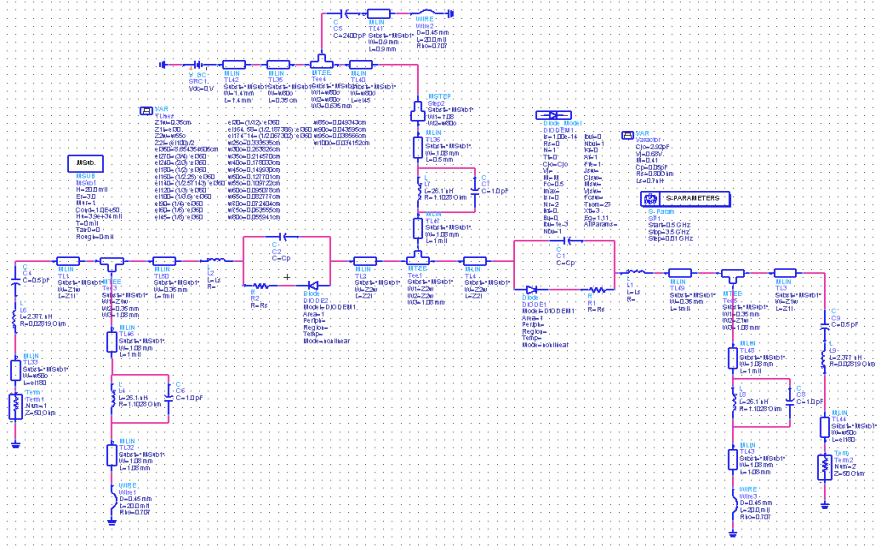
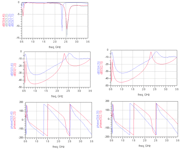
Simulations were done with the amplifier and its biasing network, the power divider, and the tunable bandpass filter. These simulations showed results for the feedback loop gain and phase. The Feedback circuit containing the amplifier, power divider, and tunable bandpass filter is shown in Figure 29. The power divider is shown as a generic three port device and is linked to a file containing the measured S-parameters for the power divider. The amplifier is shown as a generic two port device linked to the S-parameters provided by the manufacturer. The S21 parameter for the feedback circuit is shown in Figure 2. From examining the graph in Figure 30, you can see that the gain is around 6 dB to 10 dB depending on the frequency. This was a problem because for unity gain in the feedback loop, a gain of 0 dB is needed. The Distributed Amplifier is not included within the circuitry yet and it provided a gain of 10 dB.
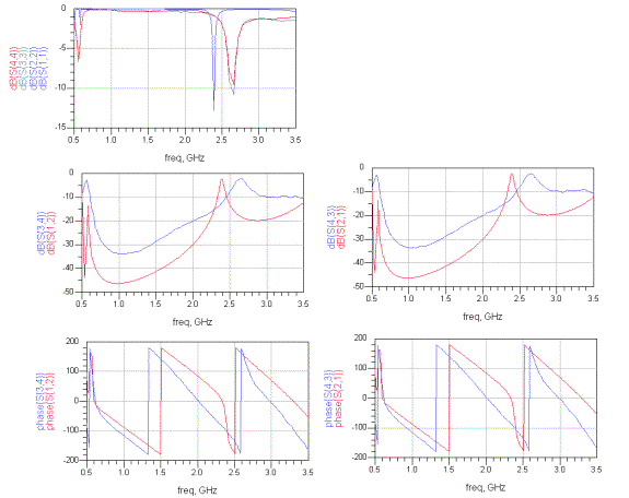
Therefore, the feedback loop circuitry in Figure 29 was re-simulated without the amplifier in the circuit. The feedback loop circuitry without the amplifier is shown in Figure 31 with the Agilent ADS simulated S21 parameter shown in Figure 32.
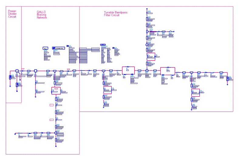
Figure 29. Schematic for the Feedback
circuitry containing the Power Divider, Amplifier biasing
network, and Tunable Bandpass Filter for
use in Feedback loop. Schematic
obtained
from Agilent ADS simulator.
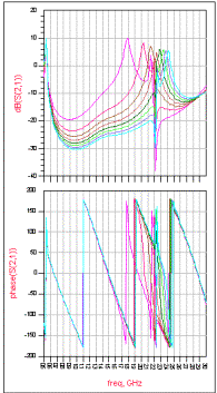
Figure 30. S12 for feedback
circuitry shown in Figure 14 from Agilent ADS simulator.
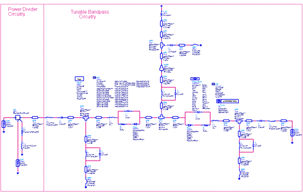
Figure 31. Feedback circuitry
containing the Power Divider and Tunable Bandpass Filter. Schematic obtained from Agilent ADS
simulator.
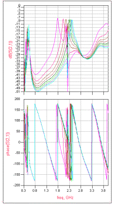
Figure 32. S12 for feedback circuitry shown
in Figure 16 from Agilent ADS simulator.
From viewing
Figure 32, you can see that the gain within any one passband is around –7 dB to –9 dB. This was fine because when the Distributed Amplifier was
connected to the circuitry it provided around 10 dB of gain. With other losses due to the microstrip
lines within the complete circuit, the overall gain was around 0 dB. This is what was desired.
Conclusions:
The
conclusion from this part of the overall project is the lack of need for an
amplifier within the feedback loop of the VCO.
This was determined by comparing Figure 32 with Figure 30. Figure 30 shows a gain greater than needed
even without the Distributed Amplifier included. Figure 32 shows a gain lower than needed but when the Distributed
Amplifier was included the gain rose up to the needed 0 dB.
For this project, a different
design was used for the tunable bandpass filter than in the previous work. This provided our team with less loses
within the feedback loop thereby eliminating the need for an amplifier in the
feedback loop.
Results Analysis
Proposal for Future Research
·
Completion of this
design iteration.
·
Examine alternative
feedback methods
·
Replace the tunable
filter with a tunable phase shifter.
·
Expand overall
system bandwidth
·
Develop a tuning
system that has a wider band of operation.
·
Design a broadband
power divider.
·
Expand the
amplifier’s bandwidth.