The Gate Level Design:
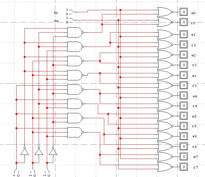
1) Address Decoder:
This address decoder selects on read and write as logic '0.' The decoder
is set up to decode through 64 bits
of storage.
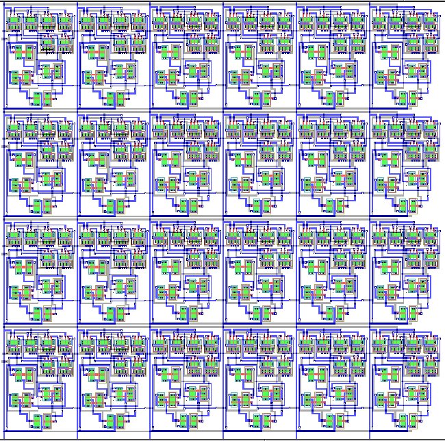
2) 8-Bit Memory Block:
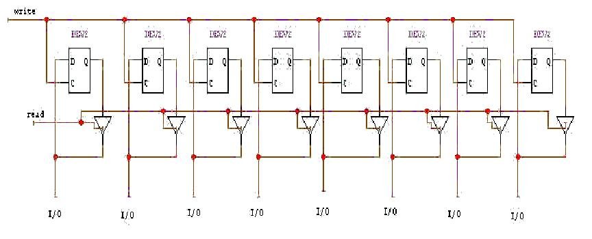
Here is a row of storage elements that uses d flip flops and tri-state
buffers. Their will be eight of these rows
so the total amount of memory stored will be 64 bits.
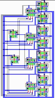
The Two Basic VLSI elements in design:
-- This example is for the storage of 30 bits because
of size constraint on the 1.2
-- micrometer pad.
Address Decoder:
This is a four bit decoder used to select which line of memory for storage.
** note: the eight bit decoder is made and will be shown during the
presentation
D Flip Flop:
This is a D flip flop made from six three-input nand gates.
Tri-State Buffer:
This is the tri-state buffer that performs the fuction of enabling a signal or not.
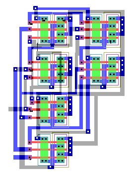
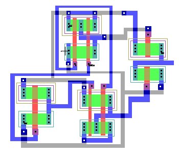
Storage Section:
Here we have the 30 bit storage section. (A combination of the D flip
flops and tri-state gates)
** note: 64 bit is implemented and will be shown during the presentation