Eric
Schultz
Advisor: Dr. V. Prasad
Risc Processor I/O
Objective
When finished, all Input/Output for a RISC processor should be designed, simulated and ready to be implemented in an FPGA. This is part of a larger project directed by Dr. Vinod Prasad to design and implement a fully functional RISC (Reduced Instruction Set) processor in an FPGA. The main objective of this project is to design the basic i/o pin structure. Possible extensions to this project are implementations of a serial port and/or an AtoD converter.
Basic Architecture
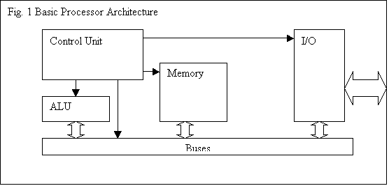
The RISC processor consists of a few main sections, these are:
- ALU – Arithmetic Logic unit
- Provides the processor with all of it’s mathematical functions (add, Subtract, Multiply, divide, And, Or….)
- Memory
- Stores Program and data for access by the processor.
- Control Units
- Sends Signals to each section to allow them to work together.
- I/O – Input/Output
- Allows Processor to send signals to external pins.
- Buses
- Paths to allow each main section to transfer data.
Description
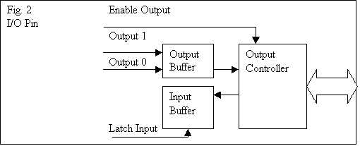
For the I/O section the most basic setup is a pin which can be set high, low, or tri-stated. This is what will first be designed. Secondly A collection of these pins (4 or 8 depending on the bus width.) will be defined for parallel transfers. Others will be defined as both bit and word addressable. All ports will be bi-directional due to the small pin count on FPGA’s. See Fig. 2
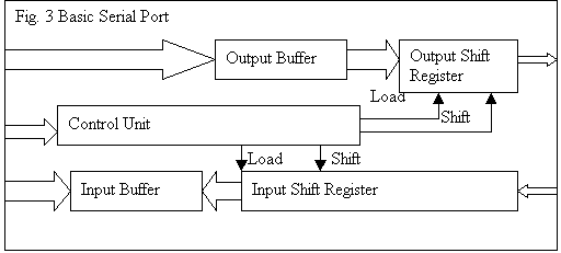
For a serial port, a timer which is available on the FPGA would be used as a baud rate generator. This would drive two shift registers which would be buffered. This would allow an easy interface to the processor. See Fig. 3.