RE-CONFIGURABLE PROCESSOR FOR COMMUNICATION
Advisors: Dr. Thomas Stewart Dr. In Soo Ahn
Students: Jared Schneider Robert
McMains
PROJECT DESCRIPTION:
This project will involve using a
Xilinx FPGA chip to implement communication modulation schemes.
The device will be re-configurable and use a modulation scheme
chosen by the operator. This reconfiguration will occur on the
fly and will occur very quickly. The modulation schemes that we
will implement into our chip will be QAM and some form of CDMA.
These modulation schemes will be implemented in digital logic,
which is downloaded to the FPGA chip from a personal computer to
a device board where the FPGA chip is mounted. This board, which
connects to the personal computer through the parallel port,
contains LED displays, toggle switches, buttons, and a bread
board type area to integrate external chips to the FPGA.
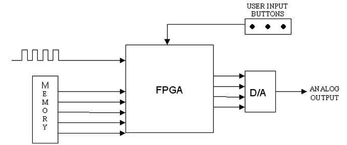
INPUTS:
Digital Input: This will be a digital signal from a function generator that we will use as our signal to be modulated.
Memory: This will be external memory that stores the data needed to reconfigure the FPGA chip to the chosen modulation scheme.
Buttons: Used to choose
which modulating scheme is implemented. They are mounted on the
board with the FPGA.
OUTPUTS:
Analog Output: The device will output a digital signal to a D/A converter and this analog output is what could be transmitted to a receiver in order to demodulate and recover the original digital input.
Figure 1. Overall System Block
Diagram
Figure 1. shows the overall system block diagram for our project. Figure 2. below shows and internal block diagram for the FPGA.
Figure 2. Internal Block Diagram of FPGA chip
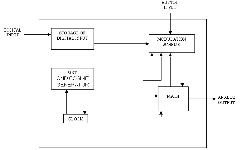
Storage: This block will hold a small portion of the digital input for use by the modulation scheme chosen.
Modulation: This block will be the configuration needed for whatever modulation scheme is chosen. It will be controlled by the button pressed as well as by the clock. This block will also use the sine and cosine generator to generate required waveforms. Finally, it can adjust the clock for the rate needed the required waveforms.
Sine/Cosine: This block will contain data necessary to create simple sine and cosine waves to be used by the modulation scheme chosen.
Clock: Used as a system clock for the modulation scheme chosen. Also used to create frequencies for sine and cosine waves.
Math: This block will contain adders, multipliers, and any other math functions needed to manipulate sine and cosine waves as well as be used by modulation scheme chosen to implement chosen scheme.