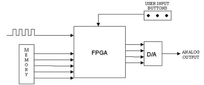
INPUTS:
Digital Input: This will be a digital signal from a function generator that we will use as our signal to be modulated.
Memory: This will be external memory that stores the data needed to reconfigure the FPGA chip to the chosen modulation scheme.
Buttons: Used to choose which modulating scheme is implemented. They are mounted on the board with the FPGA.
OUTPUTS:
Analog Output: The device will output a digital signal to a D/A converter and this analog output is what could be transmitted to a receiver in order to demodulate and recover the original digital input.
Figure 1. Overall System Block Diagram
Figure 1 shows the overall system block diagram for our project. Figure 2 below shows and internal block diagram for the FPGA.
Figure 2. Internal Block Diagram of FPGA chip
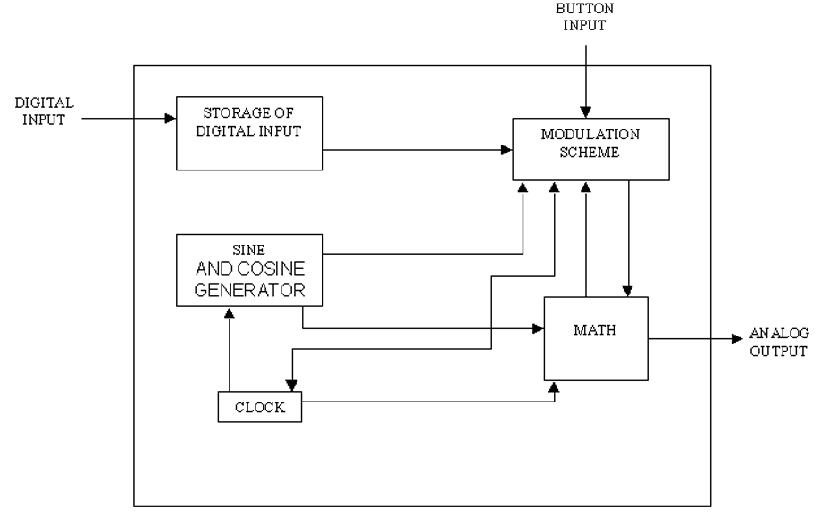
Storage: This block will hold a small portion of the digital input for use by the modulation scheme chosen.
Modulation: This block will be the configuration needed for whatever modulation scheme is chosen. It will be controlled by the button pressed as well as the clock. It will use the sine and cosine generator and change these signals to the ones needed for the modulation scheme chosen. Also, it will adjust the clock for the rate needed by the modulation scheme chosen.
Sine/Cosine: This block will contain data necessary to create simple sine and cosine waves to be used by the modulation scheme chosen.
Clock: Used as a system clock for the modulation scheme chosen, to create sine and cosine waves, and to control math block.
Math: This block will contain adders, multipliers, and any other math functions needed to manipulate sine and cosine waves as well as be used by modulation scheme chosen to implement chosen scheme.